
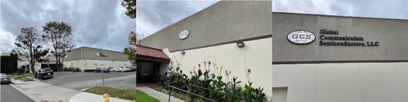
Founded in 1997, as a California Corporation, Global Communication Semiconductors, LLC ("GCS") is an ISO-certified premier pure-play compound (III-V) semiconductor (GaAs, InP and GaN ) wafer foundry service provider that manufactures technology leading, high performance, high quality, semiconductor devices. Portfolio offerings include Radio Frequency Integrated Circuits (RFIC) and millimeter wave integrated circuits for the wireless communications markets and Photodetectors and Lasers for optical communications markets.
GCS offers foundry services for RF/Wireless and Optoelectronics in addition to GCS designed proprietary optical wafers and Advanced Optoelectronics Components (AOC).
Company History
Year-Month | Milestones |
| 2018-09 | Xiamen Global Advanced Semiconductor Co., Ltd. became a subsidiary of the Company. |
| 2018-06 | The Company's board of directors passed resolution to acquire 2% of Xiamen Global Advanced Semiconductor Co., Ltd. from San'an Optoelectronics Co., Ltd. and increase the Company's ownership to 51%. |
| 2017-07 | GCS LLC acquires 100% shares of D-Tech Optoelectronics, Inc. in cash. |
| 2016-11 | Entered into joint-venture agreement with San'an Optoelectronics Co., Ltd. under which a joint-venture company Xiamen Global Advanced Semiconductor Co., Ltd., which the Company owns 49%, was established. |
| 2016-09 | Begins 6-inch VCSEL wafer fab foundry service. |
| 2016-08 | The Company's board of directors terminates the merger agreement with San'an Optoelectronics Co., Ltd. on the merger with SAIC Acquisition, Inc. |
| 2016-07 | Mass produced SiC JFET. |
| 2016-03 | The Company's board of directors passed resolution to merge with SAIC Acquisition, Inc., a 100% owned subsidiary of San'an Optoelectronics Co., Ltd. |
| 2015-12 | Successfully developed high-speed, low-loss planar RF PIN diode. |
| 2015-12 | Completed Opto foundry process developments on 100G/400G InP-PIC and INP/Si-PIC). |
| 2015-10 | Mass produced 25G 850nm GaAs PIN PD. |
| 2015-08 | Mass produced 25G 1310-1550nm PIN (25G 1310-1550nm InGaAs/InP PIN PD). |
| 2015-06 | Successfully developed high-performance Bulk Acoustic Wave Resonator. |
| 2015-04 | Established Global Device Technologies, Co., Ltd. |
| 2015-03 | Successfully developed low-loss millimeter-wave monolithic mixer diode. |
| 2014-09 | Officially listed on the Taipei Exchange. |
| 2014-03 | Successfully developed high-frequency and higher-breakdown-strength 0.15μm GaN on SiC technology and HEMT technology. |
| 2013-09 | Successfully developed high-gain, high-efficiency and high-linearity InGaP HBT for 802.11ac and 3G/4G handsets. |
| 2013-08 | Developed Super Low Noise E/D pHEMT for WLAN, GPS, DBS, and VSAT. |
| 2013-07 | Contracted with a U.S. company for GaN on SiC technology. |
| 2013-03 | Successfully developed wide band VCO HBT. |
| 2013-02 | Successfully developed high voltage InGaP HBT P7 process for the next generation of small cell base station. |
| 2013-02 | Successful certified for SiC power electric component processes from customer. |
| 2012-02 | Received order from a major international IDM plant for HBT for satellite communications. |
| 2011-10 | Successfully certified for GaN/Si high-power RF components from a U.S. company. |
| 2011-08 | Successfully transferred multiple GaAs HBT and pHEMT techniques to world-class silicon foundry company. |
| 2011-02 | Attained R&D proposal for GaN from a major international IDM. |
| 2011-01 | GCS. C became known as Global Communication Semiconductors, LLC ("GCS LLC"). |
| 2010-12 | GCS Holdings, Inc. undertook share conversion with GCS, C. |
| 2010-11 | Attained contracts for technology transfer from world-class silicon foundry for multiple InGaP HBT and pHEMT techniques. |
| 2010-11 | GCS Holdings, Inc., was established in the Cayman Islands. |
| 2008-08 | Commenced GaAs concentrated photovoltaic solar battery foundry. |
| 2004-03 | Successfully developed the world's fastest InP HBT technique (Ft > 300 GHz) that could be applied to optical communication 40-100G Trans-impedance Amplifier (TIA) and high-speed test equipment IC. |
| 2003-04 | Mass production of RF0.5µM pHEMT Switch. |
| 2001-12 | Successfully developed InGaAs PIN Photodiodes. |
| 2001-08 | Successfully developed the InP HBT technique. |
| 2001-04 | Successfully developed the high voltage InGaP HBT technique. |
| 2000-05 | Successfully developed GaAs PIN Photodiode. |
| 1999-10 | Passed ISO 9001-2000 certification. |
| 1998-12 | Successfully developed the InGaP HBT technique. |
| 1997-08 | Global Communication Semiconductors, Inc. ("GCS. C") was established and set up a facility in Torrance, CA, USA. |