Skip to header Skip to main navigation Skip to main content
Under Construction

Site branding

Home
Global Communication Semiconductors, LLC
Quality First

Main navigation

  • Home
  • About
    • Quality Policy
    • AS9100 ISO Certificate
  • Products
    • Advanced Optical Components
      • GaAs PIN Photodiodes
      • InGaAs PIN Monitor Photodiodes
      • InGaAs PIN Photodiodes
      • VCSEL Chips and Arrays
  • Services
      • Pure-Play Wafer Foundry
      • GaAs & GaN RF Wafer Foundry
      • InP HBT Wafer Foundry
      • Optoelectronics Wafer Foundry
      • Customer Proprietary Process Manufacturing
      • Processing Capabilities
      • Testing Capabilities
        • Foundry Support Flow
        • MPW Support
        • Process Design Kit
        • Testing Services
        • Foundry Training
        • Foundry Partners
      • Optoelectronics Technologies
      • GaAs Technologies
        • InGaP HBT
          • High Linearity InGaP HBT
          • High Voltage and GSM InGaP HBT
          • VCO InGaP HBT
        • Super High ƒmax HBT
        • GaAs pHEMT
          • 0.5um D-Mode T-Gate pHEMT
          • 0.25um ED mode Low Noise pHEMT
          • 0.25um D-Mode T-Gate pHEMT Power Process
          • 0.1µm Low-Noise and Power pHEMTs​
        • Integrated Passive Devices
        • THz Schottky Diode
        • Varactor Diode
      • InP HBT Technologies
      • GaN/SiC HEMT Technologies
  • Careers
    • IT System Administrator
    • Operator - 1st Shift
    • Operator - 2nd Shift
  • Contact
    • Information Request
    • Sales Request
  • News

0.25um D-Mode T-Gate pHEMT Power Process

Breadcrumbs

Breadcrumb

  • Home
  • Services
  • 0.25um D-Mode T-Gate pHEMT Power Process

Main page content

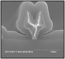
This 0.25um low cost D-Mode T-Gate process has been developed using low cost optical stepper lithography for transceiver components of up to 40 GHz and also for high operating voltage.

025um-dmode-phemt-power-process.pdf (215.19 KB)

GCS’ 0.25um T-Gate pHEMT features:

  • Low-cost optical stepper lithography process
  • Extremely high ƒmax (>200GHz)
  • Very high breakdown voltage (>20V)
 Small Signal Performance

Small Signal Performance

  • fT > 50 GHz
  • fmax > 170 GHz
  • Gmax > 14.5 dB at 30 GHz


Device
Parameters
Typical
Values
Idss (mA/mm)270
Imax (mA/mm)500
Vp (V)-1
Gm (mS/mm)350
BVgd (V)>18
  • Products
  • Services
  • Sitemap
  • Careers
  • Contact
  • ESG
  • Terms of Use
  • GCS Holdings (opens in new tab)

Copyright © 2026 Global Communication Semiconductors, LLC - All rights reserved

CMS by GCS