Skip to header Skip to main navigation Skip to main content
Under Construction

Site branding

Home
Global Communication Semiconductors, LLC
Quality First

Main navigation

  • Home
  • About
    • Quality Policy
    • AS9100 ISO Certificate
  • Products
    • Advanced Optical Components
      • GaAs PIN Photodiodes
      • InGaAs PIN Monitor Photodiodes
      • InGaAs PIN Photodiodes
      • VCSEL Chips and Arrays
  • Services
      • Pure-Play Wafer Foundry
      • GaAs & GaN RF Wafer Foundry
      • InP HBT Wafer Foundry
      • Optoelectronics Wafer Foundry
      • Customer Proprietary Process Manufacturing
      • Processing Capabilities
      • Testing Capabilities
        • Foundry Support Flow
        • MPW Support
        • Process Design Kit
        • Testing Services
        • Foundry Training
        • Foundry Partners
      • Optoelectronics Technologies
      • GaAs Technologies
        • InGaP HBT
          • High Linearity InGaP HBT
          • High Voltage and GSM InGaP HBT
          • VCO InGaP HBT
        • Super High ƒmax HBT
        • GaAs pHEMT
          • 0.5um D-Mode T-Gate pHEMT
          • 0.25um ED mode Low Noise pHEMT
          • 0.25um D-Mode T-Gate pHEMT Power Process
          • 0.1µm Low-Noise and Power pHEMTs​
        • Integrated Passive Devices
        • THz Schottky Diode
        • Varactor Diode
      • InP HBT Technologies
      • GaN/SiC HEMT Technologies
  • Careers
    • IT System Administrator
    • Operator - 1st Shift
    • Operator - 2nd Shift
  • Contact
    • Information Request
    • Sales Request
  • News

THz Schottky Diode

Breadcrumbs

Breadcrumb

  • Home
  • Services
  • THz Schottky Diode

Main page content

Monolithic THz Mixer Diode

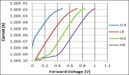
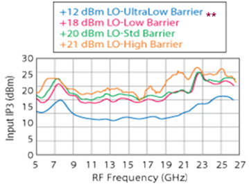
  • Schottky Diodes with fco >1 THz and Four Different Barrier Heights
  • Choice of stand-alone diode or MMIC Implementation
  • Eliminates unwanted parasitics with monolithic integration
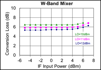
  • Low conversion loss mm-wave mixer up to W-band
  • Meets or exceeds most environmental test requirements

Process Features:

  • Planar diode process
  • Ideality factor of 1.1
  • Choice of turn-on voltage (0.3, 0.5, 0.65, and 0.85V)
  • Passive thin-film resistor, MIM capacitor and transmission lines
  • Air-bridge or polyimide interconnect options
  • Backside via option available
  • Mature manufacturing process

Applications:

  • Low conversion loss mixers
  • Up/down-converters for up to W-Band
  • Low LO drive mixer with single, multiple, series or anti-parallel diode configurations
  • Monolithically integrated options:
    • Passive matching and filtering networks
    • HBT or pHEMT integrated circuits

Electrical Characteristics:

     Model Value 
ParameterIs (fA)NRs (Ohm)Cjo (fF) @ 0.5GhzCjo (fF) @ 20GhzEstimated Fco (Thz)* 
SBD 1.6x41141.176.316.1719.711.282
SBD 1.6x61951.174.522.7627.111.305
SBD 1.6x82551.173.628.8533.211.332

 * Estimated values are obtained by using Cjo @ 20Ghz

Forward I-V Characteristics (1.6x8 mm2 diode)
W-Band Up Converter
W-Band Up Converter
Mixer Linearity
Mixer Linearity
  • Products
  • Services
  • Sitemap
  • Careers
  • Contact
  • ESG
  • Terms of Use
  • GCS Holdings (opens in new tab)

Copyright © 2026 Global Communication Semiconductors, LLC - All rights reserved

CMS by GCS