Skip to header Skip to main navigation Skip to main content
Under Construction

Site branding

Home
Global Communication Semiconductors, LLC
Quality First

Search

Main navigation

  • Home
    • About Us
    • Quality Policy
    • AS9100 ISO Certificate
  • Advanced Optical Products
    • Advanced Optical Components
      • GaAs PIN Photodiodes
      • InGaAs PIN Monitor Photodiodes
      • InGaAs PIN Photodiodes
      • VCSEL Chips and Arrays
  • Opto Foundry
      • Optoelectronics Technologies
    • Optoelectronics Wafer Foundry
  • RF Foundry
    • Overview
      • GaN HEMT
        • 0.15µm GaN-on-SiC HEMT
        • 0.25µm GaN-on-SiC HEMT
        • 0.40µm GaN-on-SiC HEMT
        • 0.25µm GaN-on-Si HEMT
      • GaAs
          • High-fT GaAs HBT
          • Super High ƒmax HBT
          • VCO InGaP HBT
          • 0.25µm and 0.5µm Power pHEMTs
          • 0.25µm Low-Noise pHEMT
          • 0.1µm Low-Noise and Power pHEMT
          • THz Schottky Diode
          • Varactor Diode
          • RF PIN Diode
        • Integrated Passive Devices
      • InP HBT
      • Foundry Support Flow
      • Process Design Kit
      • Testing Services
      • Foundry Partners
  • Contact
    • Information Request
    • Sales Request

Breadcrumbs

Breadcrumb

  • Home
  • Services
  • Pure-Play Wafer Foundry

Main page content

Pure Play Wafer Foundry

Key Aspects of a Pure-Play Foundry Model:

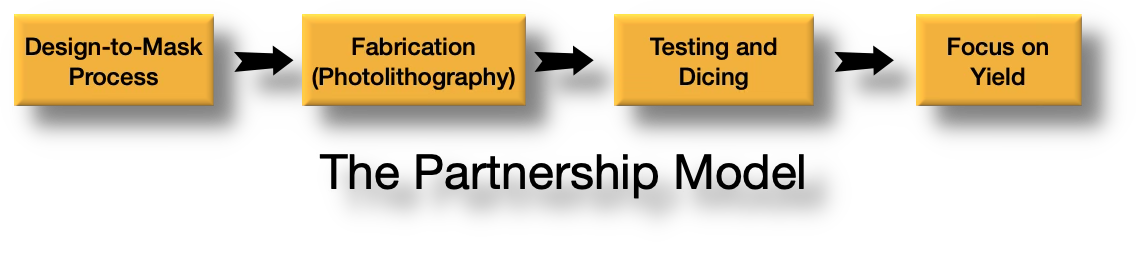
  • The Partnership Model: The foundry acts as a specialized manufacturing arm, providing the high-cost infrastructure (fabs) that clients (fabless companies) do not own.
  • Design-to-Mask Process: Clients submit finalized designs (GDSII files) using Process Design Kits (PDKs) provided by the foundry.
  • Fabrication (Photolithography): The foundry converts designs onto silicon wafers through complex, multi-month steps including deposition, etching, and ion implantation.
  • Testing and Dicing: After wafer fabrication, the foundry tests the chips and dices the wafer into individual chips (dies).
  • Focus on Yield: Foundries focus heavily on maximizing the number of working chips per wafer (yield) to reduce costs for their clients. 

Pure-play foundries thrive by providing specialized technology nodes (e.g., 3nm, 5nm) to numerous customers, reaping economies of scale that individual design firms cannot achieve on their own.

  • Products
  • Services
  • Sitemap
  • Careers
  • Contact
  • News
  • ESG
  • Terms of Use
  • GCS Holdings (opens in new tab)

Copyright © 2026 Global Communication Semiconductors, LLC - All rights reserved

CMS by GCS