
RF Semiconductor Foundry
0.1µm LN & Power pHEMT
Process Summary
Uses EBL gate lithography and is ideal for mmW transceiver components. It is suitable for commercial and aerospace & defense applications and meets or exceeds environmental requirements.
Typical Applications up to V-Band
- Transceiver Components
- High Power Amplifiers
- Low Noise Amplifiers
- Gain Blocks
- Switches
Key Features
- EBL Gate Lithography
- Excellent Reliability
- Backside Round & Slot Via Process
- Hot Via Process
- High Level MMIC Implementation
Typical Device Performance
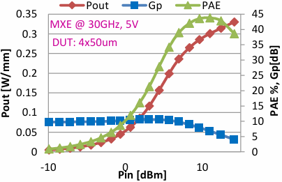
0.1µm Power pHEMT Process
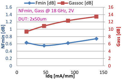
0.1µm LN pHEMT Process
Device Performance Table
| Parameter | LN | Power |
| Imax (mA/mm) | 440 | 430 |
| Idss (mA/mm) | 220 | 322 |
| Gm (mS/mm) | 430 | 383 |
| Vp (V) | -0.5 | -1.03 |
| BVgd (V) | >7 | >16 |
| fT (GHz) | 80 | 58 |
| fmax (GHz) | 170 | >210 |
| P_density (mW/mm) | NA | 630 |
| NFmin @ 6 GHz [dB] | 0.4 | 0.49 |
| Gass @ 6 GHz [dB] | 17.7 | 14.8 |
| NFmin @ 12 GHz [dB] | 0.47 | 0.76 |
| Gass @ 12 GHz [dB] | 12.5 | 10.9 |
| NFmin @ 18 GHz [dB] | 0.55 | 0.98 |
| Gass @ 18 GHz [dB] | 11.0 | 9.3 |
| NFmin @ 30 GHz [dB]* | 1.2 | N/A |
| Gass @ 30 GHz [dB]* | 9.0 | N/A |