
RF Semiconductor Foundry
0.25µm GaN-on-Si HEMT
Process Summary
Wide-Bandgap GaN on Silicon (GaN/Si) HEMT technology combining high power density, exceptional efficiency, and wide RF bandwidth. Purpose-engineered for sub-6 GHz wireless mobile systems, base station infrastructure, and Aerospace & Defense applications. This versatile process delivers stable Monolithic Microwave Integrated Circuit (MMIC) operations across a wide voltage range from 3.5V up to 48V.
Typical Applications
- Sub-6 GHz 5G Base Station Power Amplifiers
- Low-Voltage Mobile Phone PAs (5G FR1, FR3-1)
- Monolithic Integrated PA/Switch ICs for Phased Array Antenna Elements
Features
- 0.25µm Optical T-Gate Lithography with Source and Gate Field Plates
- Backside Via Process optimized for 6-Inch Wafers
Device Performance
Device Parameter Data
| Parameter | 0.25 µm |
| Imax (mA/mm) | 1050 |
| Idss (mA/mm) | 700 |
| Gm (mS/mm) | 280 |
| Vp (V) | -2.8 |
| BVgd (V) | >150 |
| MAG @ 10.0 GHz (dB) | 18 |
| ƒT (GHz) | 30.5 |
| ƒMAX (GHz) | 85 |
| MXP Psat (W/mm) @ 3.5 GHz, Vds=20V | 5 |
| MXE PAE (%) @ 3.5 GHz, Vds=20V | 81 |
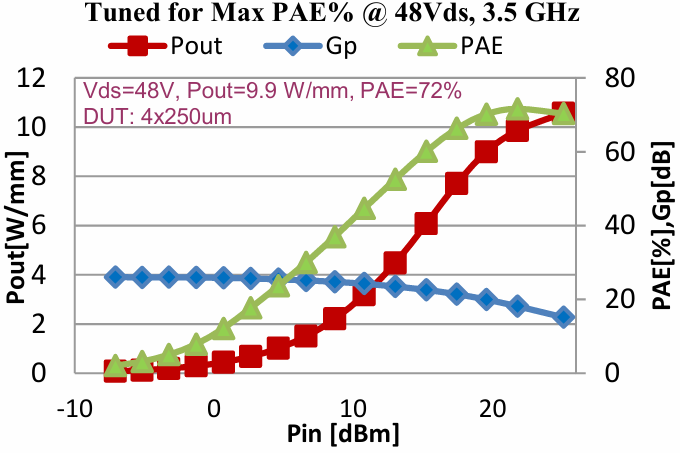
| MXP Psat (W/mm) @ 3.5 GHz, Vds=48V | 10.5 |
| MXE PAE (%) @ 3.5 GHz, Vds=48V | 72 |
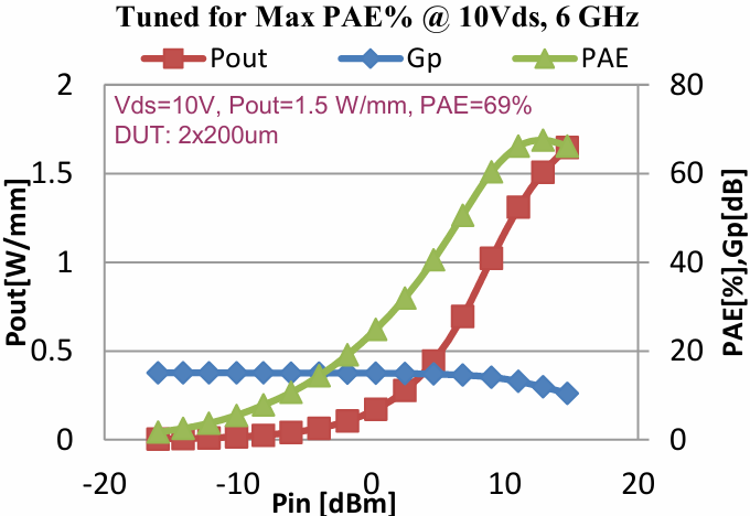
| MXP Psat (W/mm) @ 6 GHz, Vds=10V | 2.8 |
| MXE PAE (%) @ 6 GHz, Vds=10V | 69 |
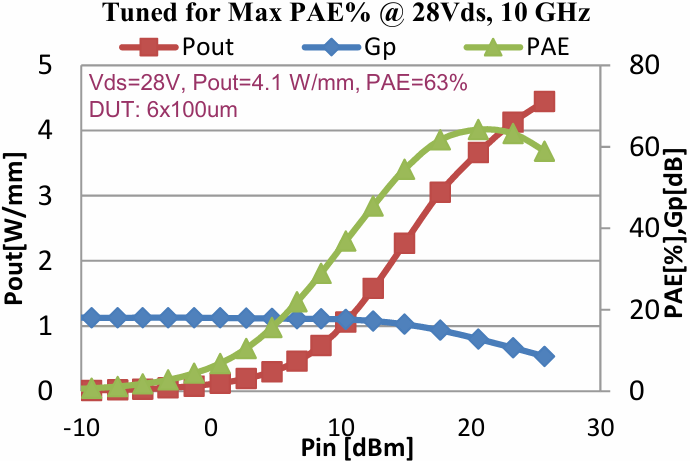
| MXP Psat (W/mm) @ 10 GHz, Vds=28V | 4.5 |
| MXE PAE (%) @ 10 GHz, Vds=28V | 64 |