
RF Semiconductor Foundry
0.40µm GaN-on-SiC HEMT
Process Summary
Wide-Bandgap AlGaN/GaN on SiC HEMT technology offering a combination of high power density, high power efficiency, and wide bandwidth. Highly optimized and ideal for sub-6 GHz 5G wireless infrastructure and radar applications across power amplifier and switch components. The process safely supports high-voltage configurations with qualified operations at 28 V, 48 V, and 85 V.
Typical Applications
- Low-band FDD PA
- Cable Television (CATV)
- Military/Commercial Radar
- Military Electronic Warfare (EW)
Features
- 0.4µm Optical T-Gate Lithography with Source and Gate Field Plates
- High Breakdown Voltage: BVdg >200V
- Excellent Thermal Conductivity
- Through-Wafer Vias
Device Performance
RF Switch Characteristics
| # Gates | Ron (Ω*mm) | Coff (fF/mm) |
| Single | 1.86 | 418 |
| Dual | 2.54 | 280 |
Device Parameter Data
| Parameter | 0.40 µm |
| Imax (mA/mm) | 1190 |
| Idss (mA/mm) | 730 |
| Gm (mS/mm) | 300 |
| Vp (V) | -2.6 |
| BVgd (V) | >200 |
| MAG @ 2.0 GHz (dB) | >24 |
| ƒT (GHz) | 19 |
| ƒMAX (GHz) | 62 |
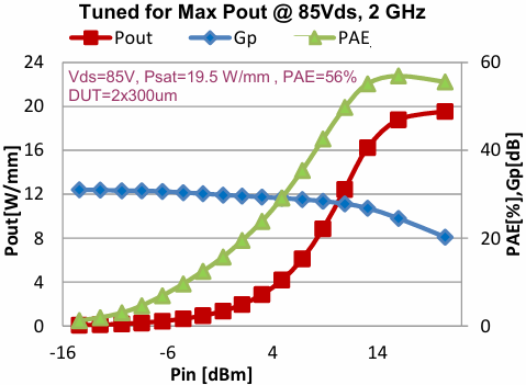
| MXP Pout (W/mm) @ 2GHz, Vds=85V | 19.5 |
| MXE PAE (%) @ 2 GHz, Vds=85V | ~75.0 |
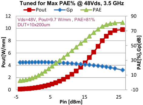
| MXP Pout (W/mm) @ 3.5 GHz, Vds=48V | 13.5 |
| MXE PAE (%) @ 3.5 GHz, Vds=48V | 81.0 |
| MXP Pout (W/mm) @ 10 GHz, Vds=48V | 10.3 |
| MXE Max. DE. (%) @ 10 GHz, Vds=48V | 57 |
| NFmin (dB) @ 10 GHz - 28V | 1.15 |