
RF Semiconductor Foundry
0.15µm GaN-on-SiC HEMT
Process Summary
Wide-bandgap GaN HEMT technology delivering a unique combination of high power density, high efficiency, and wide operational bandwidth. Optimized for high-frequency performance, it is well suited for Ku- and Ka-band and above transceiver MMIC applications. The process is qualified for 24 V, 28 V, and 40 V power amplifier operation, enabling robust and scalable RF power solutions across advanced communication systems.
Typical Applications
- mmW Transceiver Components
- Gain and Power Amplifiers
- Military/Commercial Applications
- Aerospace and Defense
Features
- 0.15µm EBL Lithography
- At 40 GHz:
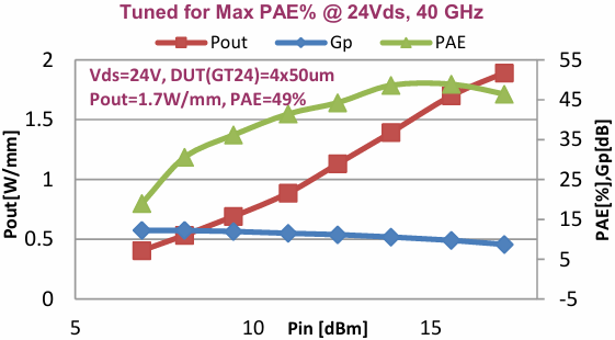
- Psat: ~5W/mm @ Vds = 24V
- PAE: 49%
- NFmin: 0.77dB @ 18 GHz
- fmax: 170 GHz
- GT40 High Breakdown Voltage: 100V
Device Performance
Device Parameter Data
| Parameter | 0.15 µm |
| Imax (mA/mm) | 1150 |
| Idss (mA/mm) | 910 |
| Gm (mS/mm) | 343 |
| Vp (V) | -3 |
| GT40 BVgd (V) | 100 |
| MAG @ 15 GHz (dB) | 16 |
| ƒT (GHz) | 42 |
| ƒMAX (GHz) | 170 |
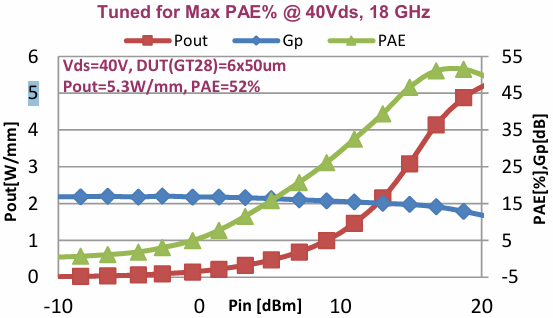
| GT40: MXP Psat (W/mm) @ 18 GHz, Vds=40V | 6 |
| GT40: MXE PAE (%) @ 18 GHz, Vds=40V | 52 |
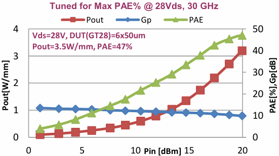
| GT28: MXP Psat (W/mm) @ 30 GHz, Vds=28V | 4.5 |
| GT28: MXE PAE (%) @ 30 GHz, Vds=28V | 47 |
| GT24: MXP Psat (W/mm) @ 40 GHz, Vds=24V | 3 |
| GT24: MXE PAE (%) @ 40 GHz, Vds=24V | 49 |
| NFmin (dB) @ 18 GHz Vds=20V | 0.77 |