Skip to header Skip to main navigation Skip to main content
Under Construction

Site branding

Home
Global Communication Semiconductors, LLC
Quality First

Search

Main navigation

  • Home
    • About Us
    • Quality Policy
    • AS9100 ISO Certificate
  • Advanced Optical Products
    • Advanced Optical Components
      • GaAs PIN Photodiodes
      • InGaAs PIN Monitor Photodiodes
      • InGaAs PIN Photodiodes
      • VCSEL Chips and Arrays
  • Opto Foundry
      • Optoelectronics Technologies
    • Optoelectronics Wafer Foundry
  • RF Foundry
    • Overview
      • GaN HEMT
        • 0.15µm GaN-on-SiC HEMT
        • 0.25µm GaN-on-SiC HEMT
        • 0.40µm GaN-on-SiC HEMT
        • 0.25µm GaN-on-Si HEMT
      • GaAs
          • High-fT GaAs HBT
          • Super High ƒmax HBT
          • VCO InGaP HBT
          • 0.25µm and 0.5µm Power pHEMTs
          • 0.25µm Low-Noise pHEMT
          • 0.1µm Low-Noise and Power pHEMT
          • THz Schottky Diode
          • Varactor Diode
          • RF PIN Diode
        • Integrated Passive Devices
      • InP HBT
      • Foundry Support Flow
      • Process Design Kit
      • Testing Services
      • Foundry Partners
  • Contact
    • Information Request
    • Sales Request

Breadcrumbs

Breadcrumb

  • Home
  • Process Design Kit

Main page content

GCS PDKs provide in-house validated device models and comprehensive layout libraries to support your designs. Available for use in Keysight ADS and/or Cadence Microwave Office (MWO), our PDKs enable accurate circuit and EM-level simulation, as well as physical verification through Design Rule Checking (DRC) and Layout vs. Schematic (LVS) validations.
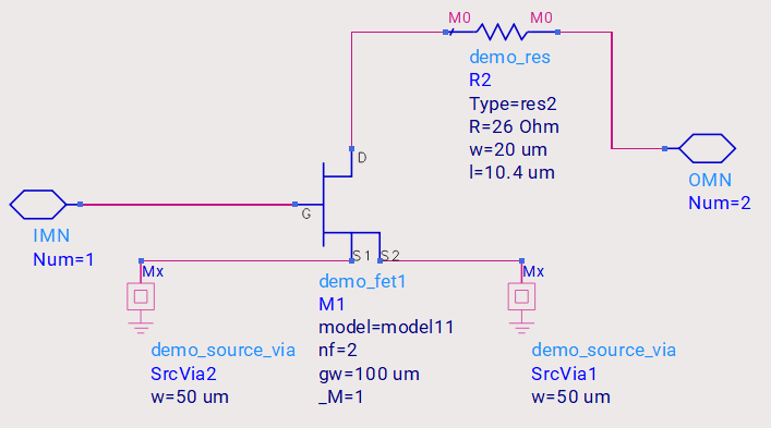
Device Models

  • Nonlinear active devices
  • Passive component devices
  • Statistical Variation parameters (Corner & Monte Carlo)
  • Advanced Thermal and Electro-thermal physics models

Schematic Symbols and Libraries

  • Fully parameterized schematic symbols
  • Technology-specific manufacturing component libraries
Schematic FET Model

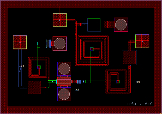
Layout PCells and Libraries

  • Parameterized Cells (PCells for transistors, inductors, MIM capacitors, and resistors)
  • Transmission Line and RF Interconnect PCells
  • Standard foundry layout cells (Pads, Backside Vias, etc.)
  • Accurate Layer definitions and standardized color maps

Technology & Process Files

  • EM Stackup multi-layer setup files
  • Substrate and GDS layer cross-maps
  • Targeted foundry process rule options

Verification Decks

  • DRC (Design Rule Check) validation modules
  • LVS (Layout vs. Schematic) geometry cross-checking
PDK Layout Automation Cells

  • Products
  • Services
  • Sitemap
  • Careers
  • Contact
  • News
  • ESG
  • Terms of Use
  • GCS Holdings (opens in new tab)

Copyright © 2026 Global Communication Semiconductors, LLC - All rights reserved

CMS by GCS