
News and Events
- GCS exhibits at IMS 2026 International Microwave Symposium (Booth #12060) at the Thomas M. Menino Convention & Exhibition Center (BCEC) in Boston, MA. June 7-12, 2026


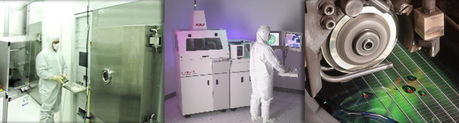
We are a semiconductor wafer foundry. We fabricate semiconductor wafers. We make our own products and we also provide foundry services for companies that do not have their own fabrication facility ("fabless").
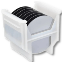
We offer foundry services for RF/Wireless and Optoelectronics in addition to GCS designed proprietary optical wafers and Advanced Optoelectronics Components (AOC).

Avoid Tariffs! We are located in the USA!
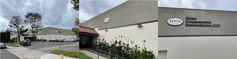
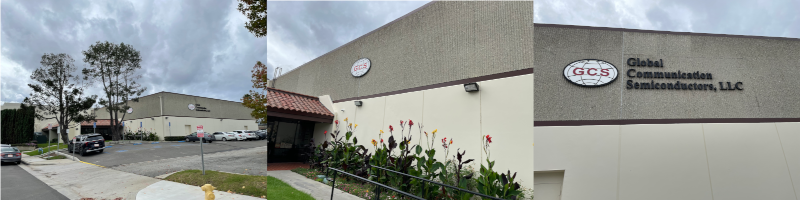
Founded in 1997, as a California Corporation, Global Communication Semiconductors, LLC ("GCS") is an ISO-certified premier pure-play compound (III-V) semiconductor (GaAs, InP and GaN ) wafer foundry service provider that manufactures technology leading, high performance, high quality, semiconductor devices. Portfolio offerings include Radio Frequency Integrated Circuits (RFIC) and millimeter wave integrated circuits for the wireless communications markets and Photodetectors and Lasers for optical communications markets.
GCS offers foundry services for RF/Wireless and Optoelectronics in addition to GCS designed proprietary optical wafers and Advanced Optoelectronics Components (AOC).
 GCS offer its own brand of high performance and high speed Active Optical Components (AOC) PIN photodetectors and Photodetector Arrays, manufactured from both GaAs and InP. Both planar and mesa photodetectors are available for applications up to 800 Gb/s with low dark current, high responsivity, and high reliability. Applications include datacom, telecom, Lightpeak, Thunderbolt, Parallel Optical Interconnects (POI), 3D Sensing and Lidar applications.
 Our Optoelectronics Products: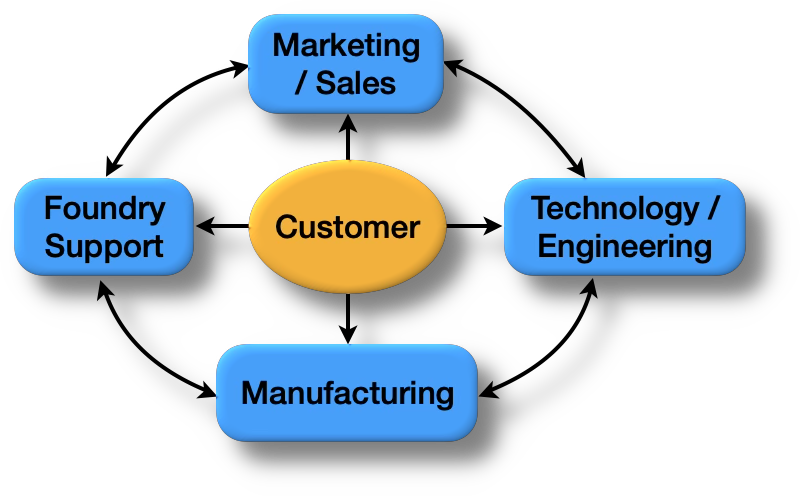
GCS was the first III-V pure-play compound semiconductor wafer foundry founded in 1997 to serve the RF wireless, millimeter wave, Optoelectronics and photonics communities. We are the experts in semiconductor devices and wafer manufacturing. We pride ourselves in providing the most intimate support to our customers. Once engaged, you will be supported by a cross-functional team from foundry support, technology and manufacturing in a customer-oriented and open innovative environment that speeds up your products from concept to volume production and time to the market.
GCS offers a comprehensive GaAs process portfolio — InGaP HBT, pHEMT, THz Schottky mixer diodes, varactor diodes, RF PIN diodes, and Integrated Passive Devices (IPD) — engineered to maximize performance across your RFIC and MMIC designs. From ultra-low phase noise VCOs to our next-generation Super-High-fmax HBT (fmax >140 GHz) for FR3 PAs up to 18 GHz, and pHEMT nodes from 0.5 µm down to 0.1 µm covering PA, LNA, and switch applications from L-band to V-band, GCS has the right process for your next design win.
When speed matters most, GCS InP HBT technology leads the industry. Our DHBT3 (fT = 290 GHz, fmax = 250 GHz) and Gen 2 DHBT3B (fT = 340 GHz, fmax = 450 GHz) processes are the foundry choice for 40G/100G TIAs, laser drivers, high-speed Mux/Demux, and mmW amplifiers — backed by proven reliability and volume production experience since 2007.
GCS GaN/SiC HEMT processes give you unmatched power density and efficiency from sub-6 GHz through Ka-band, with 0.4 µm, 0.25 µm, and 0.15 µm nodes qualified for drain voltages from 15 V to 85 V. Add our 0.25 µm GaN/Si process on 6-inch wafers for cost-effective mobile and phased-array solutions — Contact GCS today to find the right process for your next high-power RF application.
Copyright © 2026 Global Communication Semiconductors, LLC - All rights reserved