0.25/0.4/0.15µm GaN HEMT Process:
- High Electron Mobility Transistor
- Wide band-gap GaN HEMT
- A Combination of high power density, high efficiency, and wide bandwidth
- Ideal for 5G wireless infrastructure and radar applications (PA and switches)
- 15, 28, 48, and 85V PA operations
Typical Applications:
- 5G wireless infrastructures
- Amplifiers with DPD for FDD, TDD conditions
- Military/commercial radar
- Military electronic warfare (EW)
- 5G Doherty amplifier
Features:
- 0.15/0.25/0.4 µm T-Gate lithography - with source/gate field plates
- Psat: ~6 W/mm @ Vds = 28 V
- Psat: ~11 W/mm @ Vds = 48 V
- High drain efficiency: > 80%
- High breakdown voltage: > 200 V
- Excellent thermal conductivity
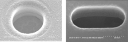
- Options of round or slot through-wafer vias
Typical GaN Device Performance:
| Parameter | 0.15um | 0.4um | 0.25um |
|---|---|---|---|
| Imax (mA/mm) | 1150 | 1190 | 1200 |
| Idss(mA/mm) | 910 | 730 | 750 |
| Gm (mS/mm) | 343 | 300 | 330 |
| Vp (V) | -3 | -2.6 | -2.4 |
| BVgd (V) | 80 | >200 | >150 |
| MAG @ 2.0 GHz (dB) | 16 | >24 | >26 |
| ƒT(GHz) | 42 | 19 | 23 |
| ƒmax(GHz) | 170 | 62 | 100 |
| Pout (W/mm)@3.5 GHz,Vds-48V | N/A | 13.5 | 11.0 |
| PAE(%)@3.5GHz, Vds-48V | N/A | 81.0 | 79 |
| Pout (W/mm)@15 GHz,Vds-28V | N/A | N/A | 4.0 |
| PAE(%)@15GHz, Vds-28V | N/A | N/A | 45 |
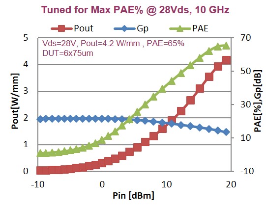
| Pout (W/mm)@10 GHz,Vds-48V | N/A | 10.3 | 10.8 |
| Max. Drain Eff. (%) @10 GHz,Vds-48V | N/A | 57 | 65 |
| Nfmin@10 GHz -28V | N/A | 1.15dB | 1.1dB |
| MXP Psat (W/mm) @ 18GHz, Vds = 28V | 5 | N/A | N/A |
| MXE PAE (%) @ 18GHz, Vds = 28V | 60 | N/A | N/A |
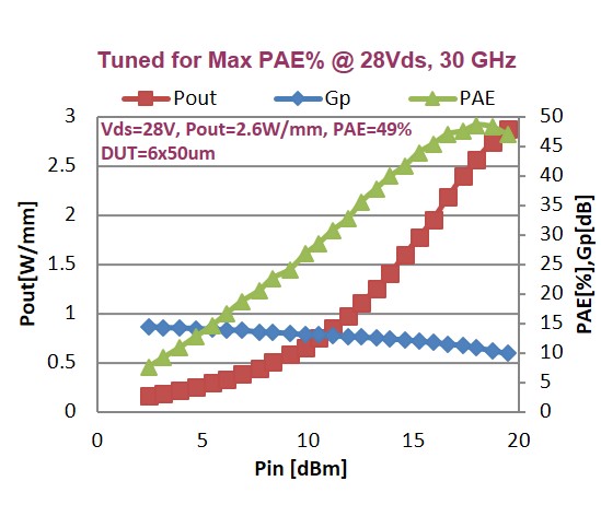
| MXP Psat (W/mm) @ 30GHz, Vds = 28V | 4.6 | N/A | N/A |
| MXE PAE (%) @ 30GHz, Vds = 28V | 49 | N/A | N/A |
| NFmin (dB) @ 18GHz, Vds = 20V | 0.77 | N/A | N/A |