
RF Semiconductor Foundry
Ultra High fT/fmax InP HBT
Generation 2
Process Summary
Our high-performance InP HBT technology delivering proven reliability across Optical Fiber Communication, Mixed-Signal, and mm-Wave applications.
Typical Applications
- Super High Speed ICs
- Mux/Demux
- 40G and 100G TIA
- 90G Static Divider
Features
- Super-High fT and fmax
- Backside Via process
Device Performance
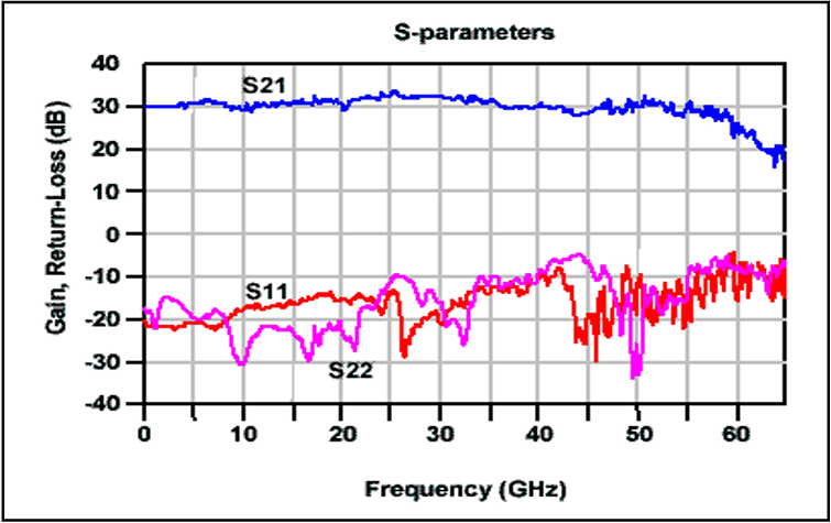 60 GHz TIA (Courtesy of SMDI)
 4:1 MUX and DMUX (Courtesy of Inphi Corp.)
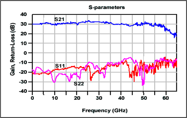 90 GHz Static Divider (Courtesy of Inphi Corp.)
Device Parameter Data
| Parameter | DHBT3 | DHBT3B GEN 2 |
| Emitter W (µm) | 0.8 | 0.6 |
| Beta | 45 | 40 |
| fT (GHz) | 290 | 340 |
| fMAX (GHz) | 250 | 450 |
| BVcbo (V) | 4.5 | 4.5 |
| BVceo (V) | 3.8 | 3.8 |
| BVbeo (V) | 3.2 | 3.2 |