
RF Semiconductor Foundry
0.25µm Low-Noise pHEMT
Process Summary
Uses optical gate lithography to enable low-cost manufacturing, with available enhancement and depletion mode options. It is ideal for LNA, gain block, and low-power digital applications, and meets or exceeds environmental requirements.
Typical Applications up to Ku-Band
- Low-Noise Amplifiers
- Driver Amplifiers
- Gain Blocks
- Transceiver Components
- Switches
- Low-power digital control function
Key Features
- AlGaAs/InGaAs/GaAs Material
- Optical T-Gate Stepper Lithography
- Low-Cost Production Process
- Excellent Reliability
Device Performance
D-Mode
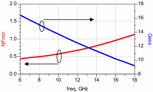
NFmin and Associated Gain (dB) of F2x75 at Vds=2V, 25% of Idss
E-Mode
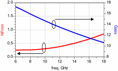
NFmin and Associated Gain (dB) of F2x75 at Vds=2V, 10% of Imax
Device Parameter Table
| Parameter | D-Mode | E-Mode |
| Imax (mA/mm) | 450 | 380 |
| Idss (mA/mm) | 175 | NA |
| Gm (mS/mm) | 440 | 560 |
| Vp (V) | -0.5 | 0.3 |
| BVgd (V) | >9 | >9 |
| fT (GHz) | >70 | >75 |
| fMAX (GHz) | >140 | >170 |
| Fmin @ 6 GHz | 0.44 | 0.25 |
| Gassoc @ 6 GHz | 16.4 | 17.3 |
| Fmin @ 12 GHz | 0.67 | 0.38 |
| Gassoc @ 12 GHz | 12.4 | 13.5 |
| Fmin @ 18 GHz | 1.14 | 0.84 |
| Gassoc @ 18 GHz | 9.2 | 10.6 |