
RF Semiconductor Foundry
0.25µm & 0.5µm Power pHEMT
Process Summary
Available in 0.25 µm and 0.5 µm process nodes, this technology uses optical gate lithography to support low-cost manufacturing. It is suited for PA, LNA, and switch applications and meets or exceeds environmental requirements.
Typical Applications up to Ka-Band
- High Power Amplifiers
- Low Noise Amplifiers
- Gain Blocks
- Transceiver Components
- Switches
Key Features
- AlGaAs/InGaAs/GaAs Material
- Optical T-Gate Stepper Lithography
- Double-Recess Gate
- Low-Cost Production Process
- Excellent Reliability
- Backside Round and Slot Via Process
Typical Device Performance
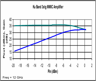 0.5µm Power pHEMT Process – Ku Band PA for VSAT
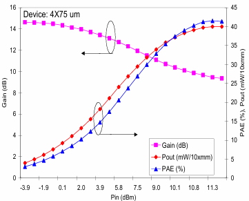 0.25µm Power pHEMT Process – Vds=6V, Vgs=-0.16V at 30 GHz
Power Performance Data
| Parameter | 0.5µm | 0.25µm |
| Imax (mA/mm) | 500 | 500 |
| Idss (mA/mm) | 250 | 270 |
| Gm (mS/mm) | 340 | 350 |
| Vp (V) | -1 | -1 |
| BVgd (V) | >15 | >18 |
| Ft (GHz) | 33 | 50 |
| Fmax (GHz) | 90 | 170 |
| P_density (mW/mm) | 900* | 650 |
* Vd=7V; Frequency=2 GHz