Skip to header Skip to main navigation Skip to main content
Under Construction

Site branding

Home
Global Communication Semiconductors, LLC
Quality First

Main navigation

  • Home
  • About
    • Quality Policy
    • AS9100 ISO Certificate
  • Products
    • Advanced Optical Components
      • GaAs PIN Photodiodes
      • InGaAs PIN Monitor Photodiodes
      • InGaAs PIN Photodiodes
      • VCSEL Chips and Arrays
  • Services
      • Pure-Play Wafer Foundry
      • GaAs & GaN RF Wafer Foundry
      • InP HBT Wafer Foundry
      • Optoelectronics Wafer Foundry
      • Customer Proprietary Process Manufacturing
      • Processing Capabilities
      • Testing Capabilities
        • Foundry Support Flow
        • MPW Support
        • Process Design Kit
        • Testing Services
        • Foundry Training
        • Foundry Partners
      • Optoelectronics Technologies
      • GaAs Technologies
        • InGaP HBT
          • High Linearity InGaP HBT
          • High Voltage and GSM InGaP HBT
          • VCO InGaP HBT
        • Super High ƒmax HBT
        • GaAs pHEMT
          • 0.5um D-Mode T-Gate pHEMT
          • 0.25um ED mode Low Noise pHEMT
          • 0.25um D-Mode T-Gate pHEMT Power Process
          • 0.1µm Low-Noise and Power pHEMTs​
        • Integrated Passive Devices
        • THz Schottky Diode
        • Varactor Diode
      • InP HBT Technologies
      • GaN/SiC HEMT Technologies
  • Careers
    • IT System Administrator
    • Operator - 1st Shift
    • Operator - 2nd Shift
  • Contact
    • Information Request
    • Sales Request
  • News

Testing Capabilities

Breadcrumbs

Breadcrumb

  • Home
  • Testing Capabilities

Main page content

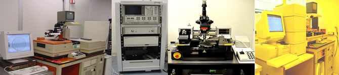
  • 100% on-wafer Automated DC and RF Testing
    • DC (die sorting)
    • RF (up to 20 GHz): OIP3, harmonics, Oscillator, S-parameters, etc.
       
  • Engineering Characterization Support (Up to 40 GHz)
    • Device Modeling (linear and non-linear models)
    • DC parametric test
    • RF small signal/large signal characterizations (load pull, OIP3, noise parameters etc.)
       
  • Automatic Wafer Mapping With Ink or Inkless Electronic Wafer Mapping

    Testing Capabilities
  • Products
  • Services
  • Sitemap
  • Careers
  • Contact
  • ESG
  • Terms of Use
  • GCS Holdings (opens in new tab)

Copyright © 2026 Global Communication Semiconductors, LLC - All rights reserved

CMS by GCS