
RF Semiconductor Foundry
0.25µm GaN-on-SiC HEMT
Process Summary
Wide-Bandgap AlGaN/GaN on SiC HEMT technology delivering a combination of high power density, high power efficiency, and wide bandwidth. Ideal for 5G wireless infrastructure and radar applications (power amplifiers and switches) running operations up to the Ku-band. The process is fully configured for robust 15 V, 28 V, and 48 V power amplifier operation.
Typical Applications
- 5G Wireless Infrastructures
- Cable Television (CATV)
- Military/Commercial Radar
- Military Electronic Warfare (EW)
Features
- 0.25µm Optical T-Gate Lithography with Source and Gate Field Plates
- High Breakdown Voltage: BVdg >200V
- Excellent Thermal Conductivity
- Through-Wafer Vias
Device Performance
Device Parameter Data
| Parameter | 0.25 µm |
| Imax (mA/mm) | 1200 |
| Idss (mA/mm) | 750 |
| Gm (mS/mm) | 330 |
| Vp (V) | -2.4 |
| BVgd (V) | >150 |
| MAG @ 2.0 GHz (dB) | >26 |
| ƒT (GHz) | 23 |
| ƒMAX (GHz) | 100 |
| MXP Pout (W/mm) @ 3.5 GHz, Vds=48V | 13.5 |
| MXE PAE (%) @ 3.5 GHz, Vds=48V | 78 |
| MXP Pout (W/mm) @ 10 GHz, Vds=48V | 10.8 |
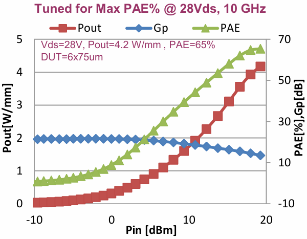
| MXE Max. DE. (%) @ 10 GHz, Vds=28V | 65 |
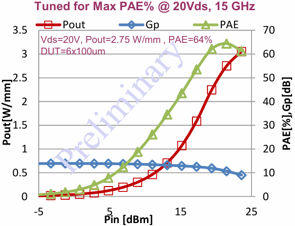
| MXP Pout (W/mm) @ 15GHz, Vds=20V | 4.1 |
| MXE Max. PAE. (%) @ 15 GHz, Vds=20V | 64 |
| NFmin (dB) @ 10 GHz - 28V | 1.1 |