
RF Semiconductor Foundry
High-fT GaAs HBT
Process Summary
This process supports a high level of integration with integrated Schottky and varactor diodes available, enabling compact RF and mixed-signal implementations. The availability of these on-chip diodes makes the technology well suited for voltage-controlled oscillators (VCOs) and high-speed ICs, while maintaining compliance with industry-standard environmental and reliability requirements.
Typical Applications
- VCO’s
- Transceiver Components
- Voltage Tunable Filters
Key Features
- Wide Tuning Range
- Low Phase Noise
- High Cut-Off Frequency
- Ideal for:
- VCO
- Prescalar/Divider/Amplifier
- OC48/192 (TIA, Laser Driver)
- Wide range tunable filter
Device Performance
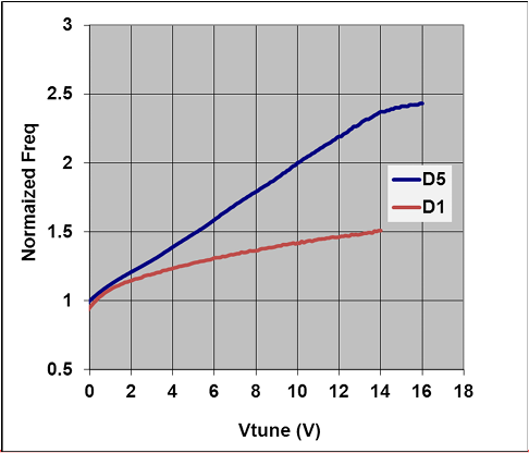 Normalized Frequency vs Vtune
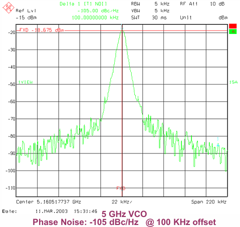 Device Performance Map
Varactor C-V Tuning Ratio
| C0V : C12V | C0V : C14V | C0V : C15V | Max Vtune (V) | Varactor Vbr (V) | |
| D1 | 2.5 : 1 | 2.7 : 1 | N/A | 13 | 17 |
| D5 | 4.7 : 2 | 5.5 : 1 | 5.7 : 1 | 16 | 29 |
Device Parameter Data
| Parameter Name | Unit | D1 | D5 |
| Base Sheet Resistance | Ω/sq | 295.0 | 295.0 |
| Collector Sheet Resistance | Ω/sq | 13.0 | 13.0 |
| Current Gain @ 1KA/cm² 14x14 | 150.0 | 150.0 | |
| Vbe-on @ 2A/cm² | V | 1.1 | 1.1 |
| Vce Offset Voltage @ IB=100µA | V | 0.1 | 0.1 |
| BVbeo @ 2A/cm² | V | 6.5 | 6.5 |
| BVceo @ 2A/cm² | V | 7.5 | 7.0 |
| BVcbo @ 2A/cm² | V | 17.0 | 29.0 |
| Ree (2x6 device) | Ω | 7.0 | 7.0 |
| Unit Cbc0V from PCMS | fF/um2 | 0.5 | 0.54 |
| Ft at 50KA/cm2 | GHz | 55.0 | 42.0 |
| Fmax at 50KA/cm2 | GHz | 65.0 | 55.0 |